New Delhi, 5 October (IANS). Union Electronics and IT Minister Ashwini Vaishnav has recently approved the establishment of ‘Namo Semacunder Laboratory’ in IIT Bhubaneswar to strengthen the country’s semiconductor ecosystem. This statement was made by the Ministry of Electronics and IT on Sunday.
The project will be provided funds under the MPLAD scheme. The estimated cost of this project is Rs 4.95 crore.
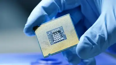
The ministry said that Namo Semacist Lab will contribute to the huge talent of India by providing industry-friendly skills to the youth. This lab will establish IIT Bhubaneswar as the center of semiconductor research and skill development. This lab will help in developing talent for chip construction and packaging units to be established across India.
This new laboratory will further promote ‘Make in India’ and ‘Design in India’ initiatives. It will act as a catalyst for India’s fast growing semiconductor ecosystem.
The government further said that this proposed laboratory will provide the necessary equipment and software required for semiconductor training, design and construction. The estimated cost of equipment is Rs 4.6 crore and the cost of software is Rs 35 lakh.
India has a 20 percent stake in global chip design talents. Students from 295 universities across the country are using the latest EDA equipment provided by the industry. The chip designed by 28 students from 20 institutes is displayed at SCL Mohali.
Odisha has recently received approval for two semiconductor projects under the India Semiconductor Mission. One of these is an integrated center for silicon carbide -based mixed semiconductor. The second advanced 3D glass is a packaging center.
IIT Bhubaneswar already has a silicon carbide research and innovation center. This new laboratory will increase existing cleaneom facilities. This will provide research and development facilities to cooperate with the semiconductor industry in India.
-IANS
ABS/


